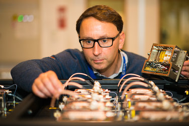
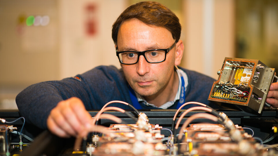
Key components of tree-counting Biomass radar cleared for space
How many trees are there on Earth? ESA’s Biomass mission will perform a global forest survey, harnessing the longest radar wavelength to pierce through woodland canopies. New microwave transistors made with the most promising semiconductor since silicon make this possible – and are now qualified for spaceflight.
Due for launch in 2022, Biomass’s five-year mission is to chart the biomass of Earth’s forests, and its changes over time. It will contribute to understanding of climate change and its effects on Earth’s system through the global carbon cycle. It does this using a ‘synthetic aperture radar’ to send down signals from orbit and record the resulting backscatter, to build up maps of tree height and volume, and sharpen estimates of global carbon stocks.
To see through leafy treetop to the trees themselves, Biomass will employ long-wavelength ‘P-band’ radar, which has never previously flown in space. It will have its signals amplified to travel down from a 600-km-altitude orbit down to Earth and back.

“This presented a technical challenge,” explains Florence Hélière, Biomass Payload Manager. “Because of the long, metre-scale wavelength of P-band radar, traditional vacuum tube power amplifiers would be far too big and heavy for the satellite.
“Instead we turned to solid state transistors as amplifiers – but no existing technology in the world provided the performance the instrument design needed. Fortunately, in parallel, another solution had become available, following years of ESA-led development.”
These alternative transistors are based on gallium nitride (GaN), hailed as the most promising semiconductor since silicon. If you own a BluRay player you own a tiny crystal of GaN, part of the violet laser diode that reads discs.
Versatile GaN’s ‘wide bandgap’ nature means it has the potential to provide 10 times more radio frequency output power than traditional semiconductors, while also operating at much higher temperatures. As a plus for space, it is also inherently radiation resistant, so can cope with the space environment including unpredictable space weather caused by the Sun.
“More than a decade ago, ESA saw the potential of GaN technology, and the importance of developing a reliable supply chain for space use,” says senior ESA technology engineer Andrew Barnes.
“The result, in 2008, was the GaN Reliability and Technology Transfer initiative – GREAT2, working with European research institutes and industry to manufacture and test space compatible GaN microwave transistors and integrated circuits. Our first GaN product flew aboard ESA’s Proba-V mission in 2013.
“That early flight-demonstration showed the Biomass team that gallium nitride was ready for them to take up. Then, in 2014, the hard work began. Building on the experience of GREAT2, supported by ESA’s Earth Observation Programme, we had to flight-qualify around 120 items in all of these 15W and 80W GaN-based power transistors to show they could meet mission requirements.”

The three-year programme that followed was the most extreme set of quality control processes imaginable. The work was undertaken for ESA by United Monolithic Semiconductors, responsible for the transistor technology, and Tesat-Spacecom, overseeing their assembly, packaging and space qualification, with Airbus Defence and Space overseeing the overall Biomass mission.
To begin with, the GaN wafer batches themselves underwent radio frequency and electrical testing, and were subjected to temperature extremes and squashed or pulled apart.
As a next step, functional circuit samples were subjected to accelerated lifetime testing, running for more than 3000 hours with no RF power output degradation to pass ‘lot acceptance testing.’
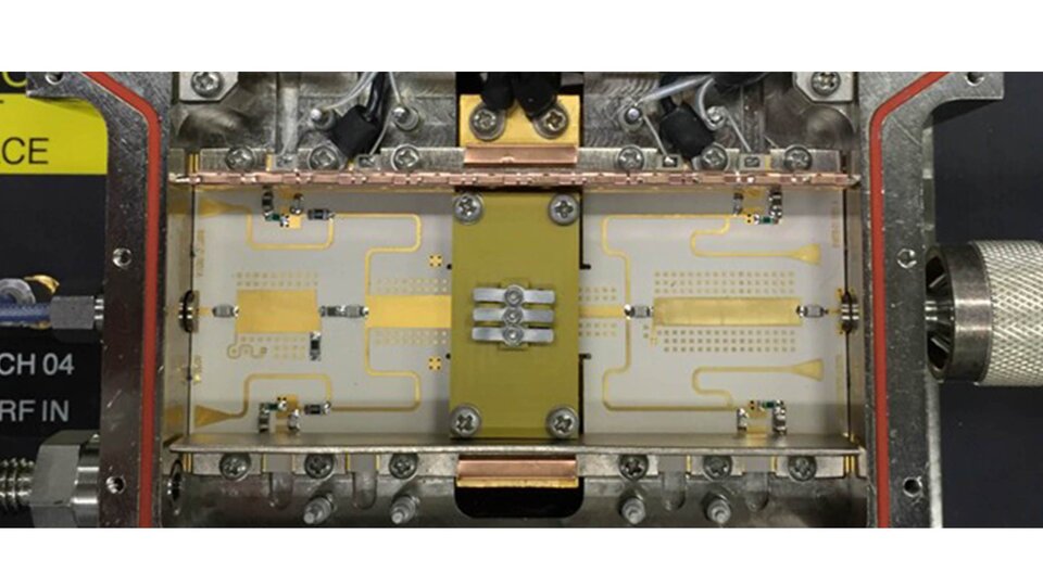
To safeguard them from the extremes of the orbital environment, the transistors needed to be fully laser-soldered within hermetic packages, followed by various tests to ensure a solid seal, ranging from X-ray inspection to hitting them and detecting the level of echo.
Once fully packaged, parts were tested at random from both the 15W and 80W qualification runs for a variety of trials such as vibration and other mechanical testing, microscopic inspection, endurance tests or signal output shape and character.
“No failures were allowed during any testing,” added Andrew, “otherwise the entire lot had to be scrapped and manufacturing restarted.”
The devices have also completed radiation testing – simulating the interaction with charged particles encountered in space – as well as for various destructive effects known to be triggered by operating high-power radio systems in vacuum.
“As a result, these GaN transistors are fully cleared for integration into the final Biomass radar instrument design,” comments Andrew, “providing the right technology at the right time for this crucial Earth-observing mission. And they are also available for other ESA and European missions in the future.”