
Method for Measuring and Viewing a Wave Surface using Spectrophotometry
| 713 - Abstract: |
| Dielectric coatings are used, for instance, to control the spectral reflectance and transmittance of a component in an optical system. The spectral phase-shift introduced by the dielectric coatings combined with manufacturing errors can affect the behavior/performance of the optical system negatively. Therefore, monitoring and/or mitigating the impact of the phase shifts on optical performance is of importance. The European Space Agency introduces an invention to help design coatings more robust to manufacturing errors and easing the assessment the spectral performance of as-manufactured components using di-electric coatings. License agreements are sought. |
Description:
It was found that the combination of the phase shift introduced by di-electric coatings and manufacturing errors can have catastrophic consequences on the end-to-end performance of optical systems. The proposed method helps designing di-electric coatings more robust against manufacturing errors by proposing an additional criterion for coating optimization. The method also helps retrieving for any wavelength the as-manufactured spectral phase-shift. Quality requirements and demanding optical performances of high precision optical instruments can be met easier.
A phase map of optical components with dielectric coatings is reconstructed with ESA’s method. The invention uses a fully parametric approach to examine the phase shift of an optical component. To reconstruct the reflected or transmitted wavefront of the system, the invention only relies on the knowledge of the as-designed phase-shift of the di-electric coating, since its design details are often retained by the coating manufacturer as part of his Intellectual Property. The theoretical phase-shift is then combined with two wavefront maps measured at two different wavelengths, so to retrieve the as-manufactured phase-shift for any arbitrary wavelength.
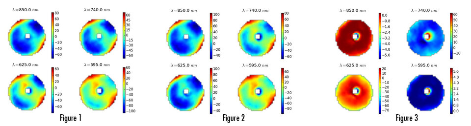
Figure 1: Measured wavefront maps in reflection.
Figure 2: Reconstructed wavefront maps in reflection.
Figure 3: Differences between as-measured and as-reconstructed wavefront maps.
Innovations and advantages:
- Reduced production costs for optical components manufactured with di-electric coatings
- Easy implementation and immediately applicable since no technology development is necessary. Part of the invention can be implemented in already existing coating design software.
- Valid for all di-electric coatings
- Minimal knowledge of coating design necessary
Domain of application:
The invention can be used for optical systems, i.e. for imaging systems, spectrometers, interferometers, etc. All domains of applications using dielectric coatings can potentially be impacted by the invention:
- Imaging (e.g. high end cameras)
- Medicine (e.g. microscopy)
- Metrology
- Science (gravitational wave observatories)
- Manufacturing (high precision optics and silicon wafers)