ESA developing deep sub-micron technology to deliver smarter satellites
Its standard field of interest may be the space beyond Earth but ESA is also currently working in inner space – the realm of the very small. The Agency has teamed up with industry to design a new generation of space-worthy microchips with transistors scaled down to under 100 nanometres.
"This is the first time that the European space industry moves from micro-scale electronics down to the sub micron -scale," explains ESA engineer Laurent Hili, in charge of the Agency's Deep Sub-Micron Technology Initiative.
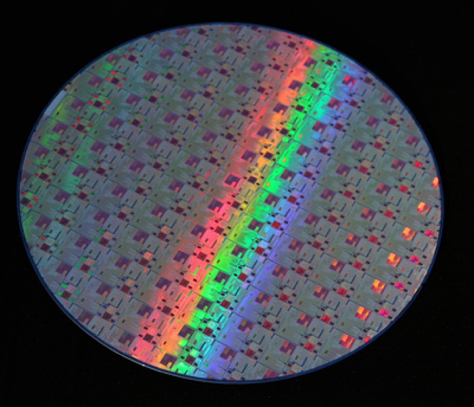
The deep sub micron -scale (below 100 nm) represents the current state of the art for the chips at the heart of the world's computers, cellphones and electronics. First engineered half a century ago, the integrated circuit has steadily gained in computing capacity by cramming ever more transistors on a single piece of semiconductor – and designers achieve this by steadily decreasing the transistor size. The result is that computers have effectively doubled in power every 18-24 months while also dropping in price – the famous Moore's Law.
ESA cannot simply buy standard computer chips for use aboard its spacecraft however – they would not survive very long. Anything placed in orbit gets bombarded by particles and cosmic rays that may damage circuits.
Instead the Agency supports design techniques for radiation-hardened integrated circuits which are certified to operate reliably for years at a time. But the space sector never stands still: the market demands smarter satellites with enhanced functionality that still remain sufficiently compact to fit standard rockets. The only way to satisfy that demand is with a new generation of more powerful integrated circuits qualified for space, which is what the Deep Sub-Micron Technology Initiative aims to deliver.
The concept of a spinning-off technology from space is well known, but this project is an example of technology 'spinning-in' from the opposite direction. "Space is only a niche in the larger integrated circuit market" says Mr Hili. "What we do is take commercial designs and adapt them for our requirements. This is something we have to do on a periodic basis, to harness market innovations for space."
Telecom satellites smartening up
Deep submicron technology should bring benefits across all space fields, but the initiative's most significant driver is the needs of the telecommunications industry, Europe's single largest and most competitive space sector.
As Mr Hili explains: "In the move from analogue to digital, telecom satellites are getting smarter. In the same way your phone is no longer just a phone but a camera, PDA, navigation device and so on, satellites are evolving into digital processors that can handle ever increasing bandwidth and numbers of channels to make more efficient use of scarce spectrum resources and deliver better services to operators and end-customers."
While computer manufacturers make do with standardised chips, spacecraft makers require customised designs to oversee different functions, known as Application Specific Integrated Circuits (ASICs). So for example, there are specific ASICs for data handling, telemetry, particle detection and star tracking among many other relevant tasks.
In practice each new ASIC is not built from scratch however but is developed by reusing a set of pre-designed building blocks known as 'cells' which collectively form an ASIC 'library'. These component cells are then placed and routed by designers on a chip to create the desired ASIC.
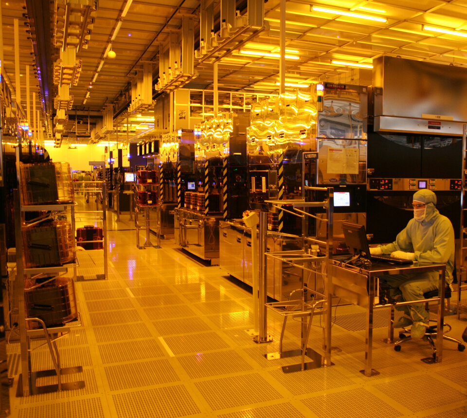
It is at these and other levels of ASIC design that ESA looks to incorporate radiation-hardening techniques, working together with industrial partners like ST Microelectronics, the fifth largest semiconductor maker in the world. Operating at the deep sub-micron scale makes this challenge more difficult still. Designers for ground applications already face problems of electrons 'leaking' out from tiny channels in this micro-world, which can cause reliability problems, but in space comes the added problem that charged particle collisions will hit with a much larger impact.
Designing for an irradiated small world
"What changes as you go to smaller scale is that the energy to flip a circuit gate from 0 to 1 gets smaller," explains Laurent Dugoujon of ST Microelectronics in Grenoble, France. "This change means the same tasks can be performed with a lower energy. But what doesn't change is the energy deposition of a heavy ion strike – so it is easier for them to trigger gate upsets, possibly affecting adjoining circuits at the same time."
To minimise the threat of such circuit scrambling means employing a number of different strategies. Analysis of ion strike consequences will guide 'hardening' actions – for example co-dependent circuit elements will get spaced sufficiently far apart so that an ion strike will only cause single errors rather than more general disruption, or else get placed on separate arrays or layers.
In addition the ASIC cells will check themselves for likely memory upsets and use counter measures such as Error Correction Codes (ECC) or Triple Modular Redundancy (TMR) with majority voting.
The current development also includes designs for High Speed Serial Links (HSSLs) – basically the express highways of integrated circuits, yielding high external throughput (Giga bits per second). And while optimised for telecom satellites, the resulting ASICs and HSSLs, integrating tens of millions of transistors per chip, will also be available to the next generation of Science, Navigation and Earth Observation missions.
The way forward
Phase 1 of the Deep Sub-Micron Technology Initiative is due to conclude in spring 2010, after which the decision will be made whether to begin trial manufacturing of the selected designs. If all goes well, the hardware could be flying by around 2014. Among the deciding factors on how to proceed, the designs will be exposed to space-like particle fluxes at ESTEC's radiation facility – radioactive isotopes of Californium-252 and Cobalt-60 can simulate high-energy ion strikes and gamma rays respectively.
The Initiative is taking place as part of the Agency element of Technology Research Programme and the European Component Initiative, an open partnership of ESA, industry and national space agencies aimed at boosting the amount of European-made electronic components that are available to Europe's space industry.
More information
Laurent.Hili @ esa.int