GREAT2 pay-offs
If successful, the pay-offs from GREAT2 will be great indeed. More capable satellites broadcasting stronger signals, coupled with improved ground terminals could extend two-way connectivity to trains, planes, cars and almost all corners of Earth.
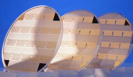
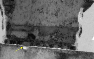
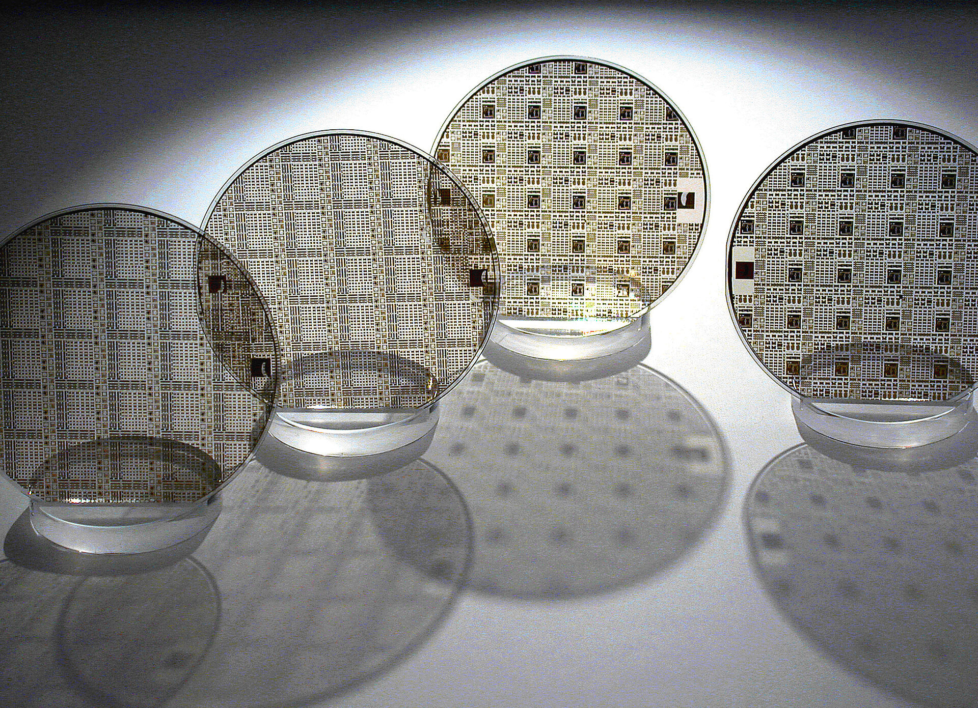
Also, the improved materials and processing knowledge gained from GREAT2 should boost Europe’s knowhow and ability to produce devices capable of operating in harsh environments. A new generation of GaN-based sensors could function without bulky shielding and operate everywhere, from the close proximity to the Sun envisaged for ESA’s Solar Orbiter mission to the radiation-soaked Jupiter system, the planned destination of a joint ESA–NASA orbiter.
The aim is to have a foundry process for space-ready microwave discrete transistors and MMICs/integrated circuits by 2011–12, with an in-orbit demonstration potentially as early as 2013.
There will be other benefits beyond the space sector, Mr Barnes concludes: “If larger silicon carbide wafers become available at affordable cost or if industry goes down the silicon substrate route, then I see no reason why GaN would not completely displace gallium arsenide. It would encompass everything from solar cells to lasers, in particular boosting the efficiency of power converters, which is a massive market, and be highly beneficial for the environment.”
Funding and coordination with other European projects
GREAT2 is being funded through ESA’s Basic Technology Research Programme (TRP) and the General Support Technology Programme (GSTP), with a larger GaN development envisaged through GSTP, the Advanced Research in Telecommunications Research (ARTES) programme and national funding.
In addition to ESA-funded activities, the Agency is coordinating GaN development with the European Commission (EC) and the European Defence Agency. The first outcome of this coordination was the launch of a complementary EC-funded Seventh Framework Programme (FP7) project, under the FP7 Strengthening Space Foundations theme, entitled ‘Advanced GaN Packaging’ (AGAPAC).
The aim of AGAPAC is to develop high thermal-dissipation packages that can be used to assemble power transistors and MMICs so that the full performance potential of GaN can be realised for space. Further complementary activities are planned; in 2009 proposals for related research, such as on substrate developments, were submitted in response to the second call of the FP7 space theme and are being evaluated.
More information
Andrew.Barnes @ esa int