What is nanotechnology?
The term nanotechnology could be at moment as fanishionable as loose. For those who are not familiar with this concept we have written a brief review.
The prefix nano comes from to the Greek nanos, meaning dwarf. In science, the prefix nano refer to one billionth (i.e. 10-9) of a unit. There is actually a cousin word of the term nano which has been used more widely: nanno (nanno), whose sense has changed from the name of the muse of the Greek poet Mimnermus (VII century BC), to a cheese cake with olive oil (II AD) and a washing basin (III AD). Nanno was used in a scientific context for the first time in 1908 (classification of small organism by Lohmann) [1]. Apart from this biological branch, the prefix 'nano' was first used in 1956 when talking of inert material and officially recognized in 1960 at the 11th Conférence Générale des Poids et Mesures (Résolution 12) [2]. But in the space sector, where big telecommunication satellites weight several tons, a nanosatellite usually refers to a spacecraft with a mass between 1 and 10 kg.
The long-ignored Feynman talk "There is Plenty of Room at the Bottom" [3], in December 1959, was an attempt to attract the attention of scientists to a world of nanomachines made of a few hundreds of atoms. He challenged the community to create an electrical motor "smaller than 1/64th of an inch" (roughly 400 um). However, to his consternation, the winner Willian McLellan accepted this defy, but working at a macroscale level, using tweezers and microscope [4].
Top-down vs. bottom-up approaches
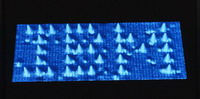
The top-down approach is the one usually used in microtechnology, where microsystems are built thanks to photolithography, thin film deposition and selective etching. And actually, this is also the approach of Feynman, when he envisioned big machines building smaller ones, which would build smaller ones and so on. On the contrary, nanotechnology focuses on the bottom-up approach, and start to build structures atom by atom. A very famous picture demonstrating nanotechnology capability is the spectacular image from [5] showing the letters IBM written with xenon atoms on a nickel surface (see below) thanks to a scanning tunneling microscope.
But actually, moving atoms one by one is a fairly long process and any practical device would require an enormous and unrealistic amount of time to be built. Therefore, researchers are working on some processes of self-assembly [6, 7] or massive parallel manipulation of single particles [8]. One specificity of nanotechnology is that at this level (a nanometer corresponds to roughly the diameter of 9 atoms of silicon), quantum effects appear that have to be taken into account or better, that can be exploited. But the border between micro and nanotechnology is quite porous, with for instance tunneling effect already used for commercial NAND flash memory.
The "nano" word: a fashion victim
Nowadays, many research groups are using the prefix nano because the word is very popular and seems to attract funding from institutions and companies who are afraid to miss the so-called "3rd industrial revolution". Nanotechnologies are defined by the Royal Society as the design, characterisation, production and application of structures, devices and systems by controlling shape and size at nanometre scale while nanoscience is the study of phenomena and manipulation of materials at atomic, molecular and macromolecular scales, where properties differ significantly from those at a larger scale [9]. In [1] C. Joachim demands that "nanoscience should be reserved solely for the study of a single atom or a single molecule, that is, of one entity at a time, and not for groups of such entities where statistics or interactions between them come into play."
Nanoscale science: a multidisciplinary field
Wanting to be somewhat broader than C. Joachim, it has to be noted that when we refer to nanotechnology, we actually refer to a more general "nanoscale science". Nanoscale science is at the cross-road of many disciplines, involving chemistry with the synthesis of purposely-designed molecules, physique (e.g. quantum effects) and biology (e.g. use of DNA as template molecules or liking bridges).
References
- To be nano or not to be nano?, C. Joachim, Nature Materials, 4, 107 (2005)
- Resolution 12 of the 11th Conférence Générale des Poids et Mesures (CGPM) link
- There's Plenty of Room at the Bottom - transcript of Richard Feynman's classic talk link
- Nanoelectromechanical systems face the future, M. Roukes, Physics World, 14 (2001) link
- Positioning single atoms with a scanning tunneling microscope, D.M. Eigler, E.K. Schweizer, Nature, 344, 524 (1990)
- Optimized Interactions for Targeted Self-Assembly: Application to a Honeycomb Lattice, M. C. Rechtsman, F. H. Stillinger, and S. Torquato, Phys. Rev. Lett., 95, 228301 (2005)
- Self-assembly of base-functionalized carbon nanotubes, C. Song, Y. Xia, M. Zhao, X. Liu, B. Huang, F. Li and Y. Ji, Phys. Rev. B, 72, 165430 (2005)
- Self-assembly of base-functionalized carbon nanotubes, C. Song, Y. Xia, M. Zhao, X. Liu, B. Huang, F. Li and Y. Ji, Phys. Rev. B, 72, 165430 (2005)
- Nanoscience, and Nanotechnology: Opportunities and Uncertainties, Document 19/04, The Royal Society, London (2004) link