ESA probing into post-silicon, wide bandgap landscape
What comes next after silicon? Some seven decades from the invention of the silicon chip this question is often asked, especially in the space sector: demands for extreme high performance have highlighted silicon’s inherent limitations, raising interest in a new range of ‘wide bandgap’ semiconductor materials.
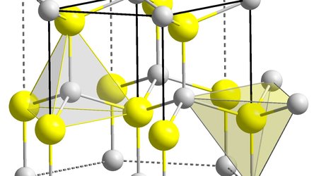
A material’s ‘bandgap’ is the space between atomic shell layers that dictates the amount of energy needed to get electrons moving and make that material conductive. But electrons can also be shifted into the conduction band by heat; so, for instance, silicon-based semiconductors become unusable for temperatures from around 180°C and up.
Wide bandgap materials such as gallium nitride, silicon carbide and diamond can attain much higher operating temperatures, potentially enabling much higher current density designs running at higher voltages. Electrons also move faster through them, delivering faster device speeds. And as an added benefit they are robust against the effects of radiation – a particular issue in space.
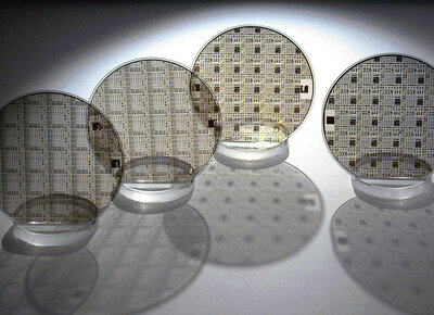
ESA recognised the potential of the wide bandgap realm for space at an early stage, founding the ‘GaN Reliability Enhancement and Technology Transfer Initiative’ (GREAT2) in 2008 for gallium nitride (GaN) microwave devices, at a time when it was used mainly for high-performance LEDs and the lasers of Blu-ray players.
Leading research institutes were brought together with manufacturers to set up an independent European supply chain to manufacture high-quality GaN radio frequency devices for space applications.

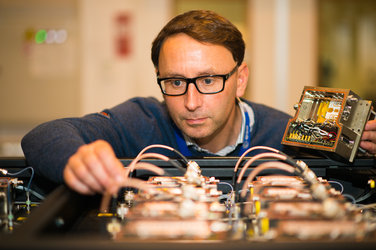
“The promise of these materials makes them highly strategic,” explains Andrew Barnes, heading GREAT2. “We need independent European supply chains because if we were totally dependent on a foreign source that became subject to export restrictions then the whole industrial sector would be compromised, along with our competitiveness.”
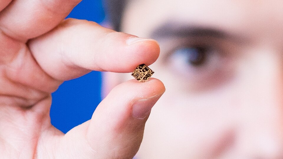
The initial focus of GREAT2 was on GaN-based microwave power transistors and integrated circuits, as building blocks for high-performance solid-state power amplifiers, to bolster the competitiveness of the European telecommunications industry – the single largest and most commercial space sector.

“These same power transistors shall in the near future be offered on the open market after completion of a project funded by ESA’s European Component Initiative, which is the first time we’ve achieved that,” adds Andrew. “Such power transistors are also being investigated for use in the next-decade Galileo Second Generation.
“At the same time we’re in the process of qualifying some of the foundry processes used on a more systematic basis, following European Cooperation for Space Standardization rules. We’re also seeking to develop additional standards in terms of screening and testing and insertion into space systems – this is essential for wider industrial take-up of the technology, and we’re making steady progress.”
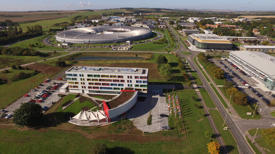
GREAT2’s focus has now moved to high voltage power converters and amplifiers for higher frequencies, operating at millimetre wavelength. The Ninth Wide Bandgap Workshop hosted at ESA’s Harwell centre in the UK took stock of the general progress made and looked ahead to the next steps towards the wide bandgap future.
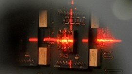
“This includes improving production quality of GaN ‘epitaxy’ – meaning crystal growth – and moving to higher frequency foundry processes for space ready parts, utilizing 100 nanometre gate lengths or lower for GaN,” explains Andrew. Work is also ongoing to test the space radiation robustness of GaN power transistors for DC-DC convertor applications.
“We’ve also worked to boost their general robustness. We found, for instance, that some of the passive components used on GaN monolithic microwave integrated circuit parts weren’t performing so well in radiation testing as expected, and this came down to the legacy of their design, originally these capacitor designs were based on legacy parts built in gallium arsenide. By tuning design parameters, i.e. adjusting the dielectric layer stack, we have now achieved a big improvement.”
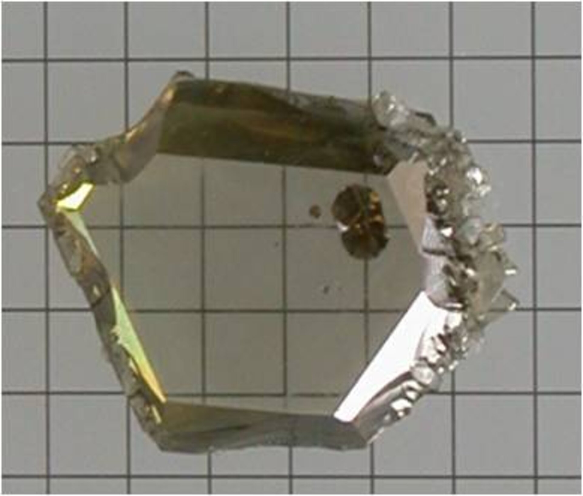
Other wide bandgap materials such as diamond are also under investigation, in their own right and also as a ‘substrate’ backing material for GaN devices to give improved thermal performance.
Andrew comments: “Diamond has a similar crystalline structure to GaN, and excellent thermal conductivity properties. The University of Bristol presented work done in integrating GaN with diamond. The result is a fivefold increase in heat dissipation, allowing even higher power densities – diamond is a GaN’s best friend.”
The workshop also peered further into the future, with discussions looking forward to GaN-based optoelectronic devices, diamond-based integrated circuits and electric thrusters and the 3D printing of wide bandgap materials, as a means of revolutionising device manufacturing.