Silicon brains to oversee satellites
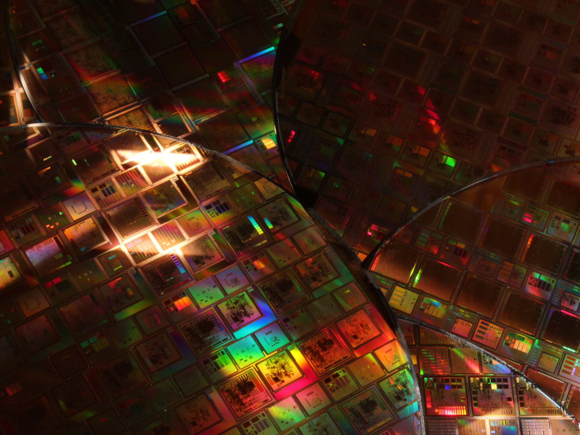
A beautiful and expensive sight: upwards of €6 million-worth of silicon wafers, crammed with the complex integrated circuits that sit at the heart of each and every ESA mission. Years of meticulous design work went into these tiny brains, empowering satellites with intelligence.
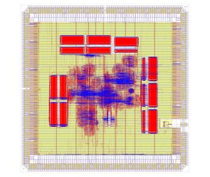
The image shows a collection of six silicon wafers that contain some 14 different chip designs developed by several European companies during the last eight years with ESA’s financial and technical support.
Each of these 20 cm-diameter wafers contains between 30 and 80 replicas of each chip, each one carrying up to about 10 million transistors or basic circuit switches.
To save money on the high cost of fabrication, various chips designed by different companies and destined for multiple ESA projects are crammed onto the same silicon wafers, etched into place at specialised semiconductor manufacturing plants or ‘fabs’, in this case LFoundry (formerly Atmel) in France.
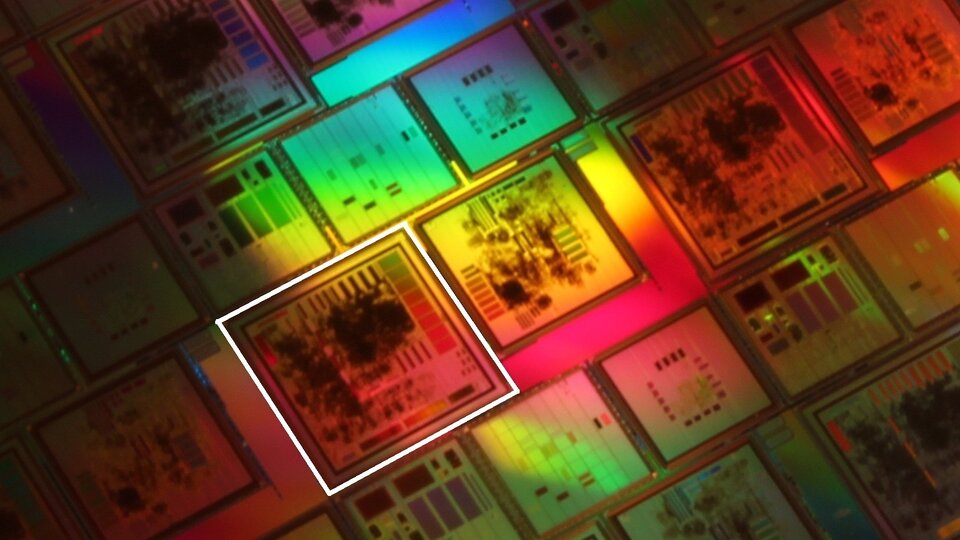
Once manufactured, the chips, still on the wafer, are tested. The wafers are then chopped up. They become ready for use when placed inside protective packages – just like standard terrestrial microprocessors – and undergo final quality tests.
Through little metal pins or balls sticking out of their packages these miniature brains are then connected to other circuit elements – such as sensors, actuators, memory or power systems – used across the satellite.
Considering the time and money needed to develop complex chips like these, ESA’s Microelectronics section maintains a catalogue of chip designs, known as Intellectual Property (IP) cores, available to European industry through ESA licence.
Think of these IP cores as the tiniest mission ‘building blocks’: specialised designs to perform particular tasks in space, laid down within a microchip.
These IP cores range from single ‘simpler’ functions such as decoding signals from Earth to control the satellite to highly complex computer tasks such as operating a complete spacecraft.
The latter is achieved for example by the SCOC-3 ‘spacecraft controller on a chip’ developed by ESA and Astrium, which itself combines more than 20 different IP cores from other sources, seen at the bottom of the image.
Each IP core is coded in a ‘hardware description language’ that can then guide the manufacturing process. Today’s state-of-the-art minimum sizes of integrated circuit tracks are measured in tens of nanometres.