


 Germany
 Austria
 Belgium
 Denmark
 Spain
Spain
 Estonia
 Finland
 France
 Greece
 Hungary
 Ireland
 Italy
Italy
 Luxembourg
 Norway
 The Netherlands
 Poland
 Portugal
 Czechia
 Romania
 United Kingdom
 Slovenia
 Sweden
 Switzerland


Focal Plane Assembly Technology Development for SPICA/SAFARI
| Programme: | GSTP | Achieved TRL: | 3, 4, 5 |
| Reference: | G512-010AP | Closure: | 2016 |
| Contractor(s): | STICHTING RUIMTE ONDERZOEK (NL) | ||
Cryogenic instruments based on imaging arrays of superconducting Transition Edge Sensor (TES) detectors operating at very-low temperature are proposed or considered for future high- and low-energy astrophysics space missions, including the X-IFU instrument for Athena and the SAFARI instrument for SPICA. In the case of both x-ray and far-infrared spectrometers, 2-dimensional arrays of 1000's of TES detectors operated at a 50 mK base temperature are used to realize high-sensitivity imaging with high optical efficiency and fast response.
TES detectors and their SQUID amplifiers are extremely sensitive to magnetic fields, and magnetic shields are a key element in the FPA design. Key requirements on these magnetic shields are to suppress the static field in the vicinity of the FPA to ~ 1 μT or less normal to the plane of the TES detector and temporal modulations in this field (e.g. linear drifts in the stray-field from a 50 mK ADR refrigerator and modulations in the stray-fields of compressors that drive mechanical cryo-coolers).
2-D arrays of 1000's of TES detectors at 50 mK enable high-sensitivity imaging with high optical efficiency and fast response. The detectors are operated using frequency division multiplexed SQUID amplifiers that offer the low input noise and input impedance required for TES readout, with a low power dissipation to fit within the limited cooling powers available at low temperatures. The TES detectors and their SQUID readout electronics are to be integrated inside Focal Plane Assemblies (FPAs) that isolate the detectors and their readout electronics at 50 mK from their environment.
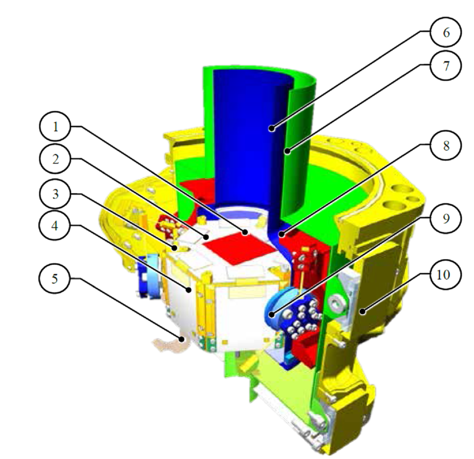
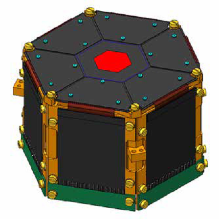
The image on the right shows the conceptual design of a TES focal plane assembly for a far-IR imaging FTS spectrometer for SPICA-SAFARI. (1) TES array, (2) TES mount with hexagonal wafer on top, (3) superconducting flexible interconnect, (4) LC resonator unit, including LC filters and SQUID amplifiers, (5) 50mK to 2K cryo-harness, (6) Nb magnetic shield, (7) Cryoperm (8) intermediate 300 mK stage, (9) Kevlar suspension unit, and (10) external housing.
Objectives
A preliminary concept for one of the far-IR TES FPA's in SAFARI. A similar design concept is considered for the TES FPA in the X-IFU instrument. This project has focussed on three enabling technologies for a TES FPA:
a) Magnetic shields to suppress spurious detector signals due to background magnetic fields;
b) High-density flexible interconnects to connect a large-format TES array with its FDM-multiplexed SQUID readout; and
c) A first demonstration of the mechanical integration of a large-format TES detector array and its 50 mK readout electronics.
Shielding factor verification
Previous work within an NL-funded activity led to the development of both a design and prototype hardware for a two-layer magnetic shield to address these two requirements. A superconducting (Niobium) shield, located at the 50 mK level, is used to suppress variability in the magnetic field environment by a factor of ~ 104 after the shield is cooled to cryogenic temperatures (below the superconducting critical temperature of Nb, Tc ~ 9 K). The Nb shield is surrounded by a mu-metal shield (typically manufactured using Cryoperm). The primary function of this Cryoperm shield is to suppress the static external field by a factor of ~ 100 so that the Nb shield can be cooled in a low-field environment, as the expectation is that the field that is present during cooldown will be frozen into the Nb when it passes through its Tc. However, the details of that process depend upon the dynamic behaviour of the superconducting phase transition of the Nb shield, which may be affected by the manner in which the Nb shield is cooled down.
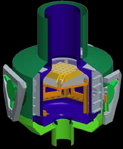
The picture on the left shows the preliminary concept of a FPA magnetic shield. A mu-metal Cryoperm shield (green) at 2 K suppresses the static external field, while a superconducting Nb shield (blue) at 50 mK provides a shielding factor of ~ 104 versus modulated fields. The achievable shielding is strongly dependent upon the shield geometry, in particular on the dimensions of the optical aperture. The Cryoperm shield reduces the field that is frozen in when the Nb passes through its superconducting transition temperature, ~ 9 K. The Nb shield is suspended inside the Cryoperm shield by a two-layer Kevlar suspension system and the detector assembly is located inside the Nb shield.

The graph on the right shows a key measurement result from TN 2.2 - the measured attenuation of a modulated external field perpendicular to the axis of the shield apertures, measured as a function of position along the axis of the shield. The measured on-axis attenuation for both an isolated Nb shield and the integrated Nb + Cryoperm shield agrees very well with finite element models of the shield configurations in Comsol. This result is true both when the shields are cooled down in zero external field, and when a static axial or transverse external field is applied during cooldown. The good agreement between measurement and model provides confidence that the finite element models can be used to predict both the off-axis performance of this shield and the performance of similar shields if design changes are needed in the future.
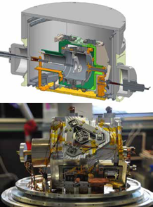
The pictures to the left show the experimental setup for measurements of the static field frozen into the integrated B-shield during cool-down. The drawing displays the assembly mounted in a LHe-cooled vacuum cryostat, with a heat-switch for controlling the Nb shield temperature and a mechanical feedthrough to allow the flux-gate magentometers to be moved, e.g. to sample the plane of the detector array. The picture below shows the assembly of the cryoperm and Nb B-shields integrated with a Kevlar suspension.
Interconnect concept
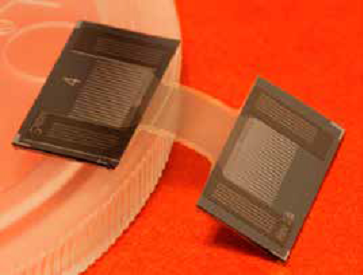
A novel "coil-coupled" interconnect concept is considered to address these requirements, combining a superconducting flex circuit (for a low resistance "around-the-corner" connection) with bump-bonding to the LC filters and a re-workable transformer-coupled connection to the TES chip. Essential elements are superconducting flex circuits terminated on bulk Si (for coil patterning and bump-bonding), a reworkable interconnect-to-TES connection, and demonstration of a transformer-coupled TES. The first two points are addressed here. Fixed transformers are used to impedance-match TES and LC filters in the SRON FDM at SRON, while a transformer-coupled interconnect demonstration will follow the developments here.
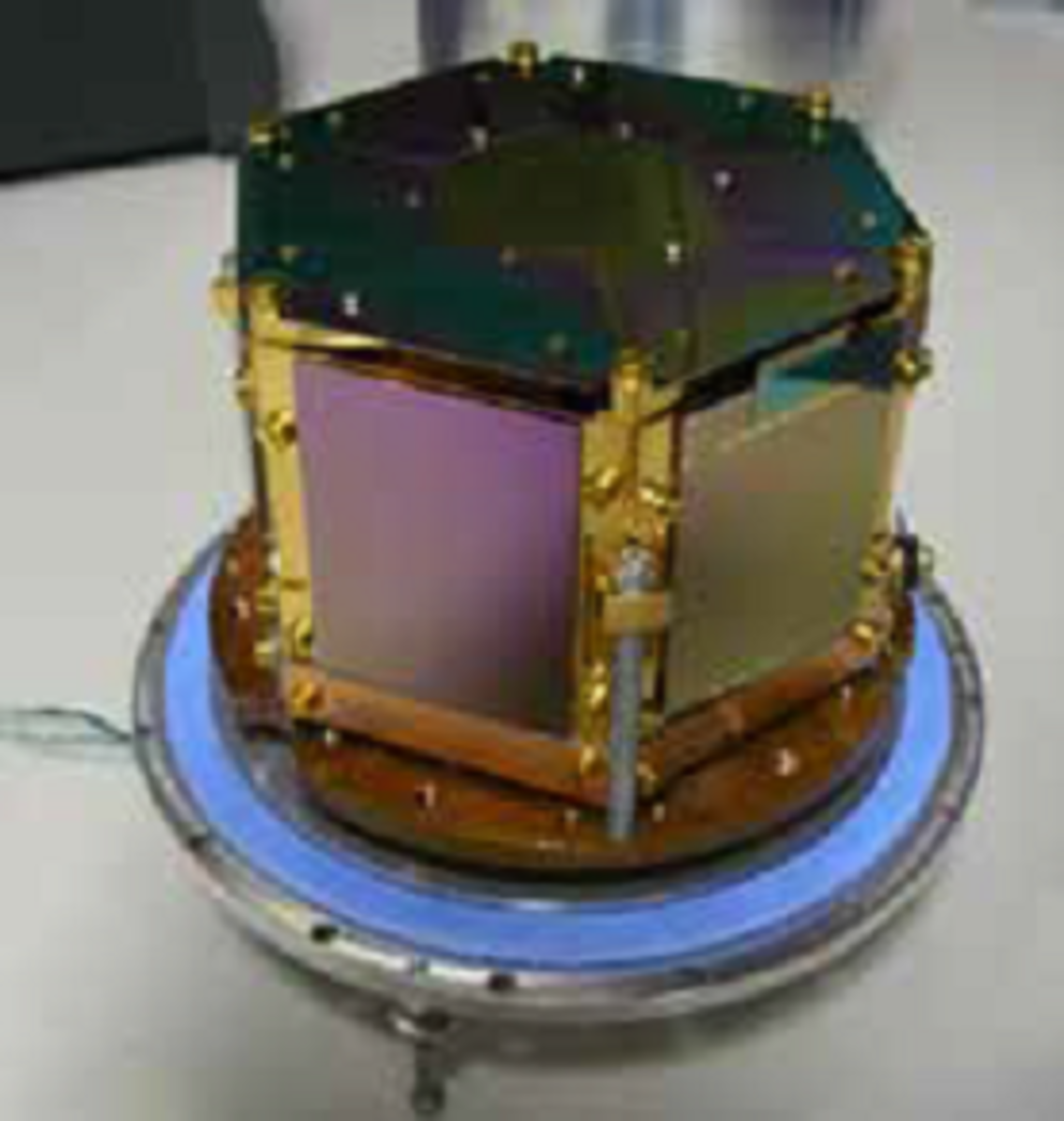
Mechanical prototype of a 50 mK detector and readout electronics assembly
A prototype 50 mK detector and readout assembly was developed (figure below) to verify its manufacturability and robustness vs. thermal cycling and random vibration. One prototype LC filter + flexible interconnect assembly was included, plus mass dummies for the remaining LC and interconnect chips. The TES chip is a structural dummy, including the silicon support grid for the TES pixels but no active pixels. Once assembled the 50 mK mechanical prototype was thermally cycled 20 times to ~ 80 K, with no visual damage observed (see figure at the top of this article). Following the thermal cycle test, the assembly was vibration tested.
Low-level sine sweeps were used to verify the assembly's stiffness and check integrity before and after vibration tests. Random vibration tests were performed using spectra scaled in amplitude from preliminary estimates of qualification loads, starting at a low level and ramping up to the nominal test level (0dB). No damage was observed after the 0dB test, so testing continued to characterize the design's margins. The assembly survived a +3dB test, but the glue spots fixing the TES wafer to its support failed at +6dB.
Application
Used in X-IFU (ATHENA) and/or SAFARI (SPICA)
Further activities
For the B-shield, points to address in the future include a) testing the cryoperm shield at higher modulation frequencies, b) further developing the magnetic bias coil and c) reviewing the instrument (X-IFU/SAFARI) instrument requirements.
For the TES-to-LC interconnect ongoing work is needed to pinpoint and resolve the degradation of superconductivity in the narrow Nb lines in the flexible interconnect process.
For the 50mK prototype further design optimizations for assembly are desired, as is fine-tuning to address damage to the TES wafer due to contact with the interconnect chips during vibration.