


 Germany
 Austria
 Belgium
 Denmark
 Spain
Spain
 Estonia
 Finland
 France
 Greece
 Hungary
 Ireland
 Italy
Italy
 Luxembourg
 Norway
 The Netherlands
 Poland
 Portugal
 Czechia
 Romania
 United Kingdom
 Slovenia
 Sweden
 Switzerland


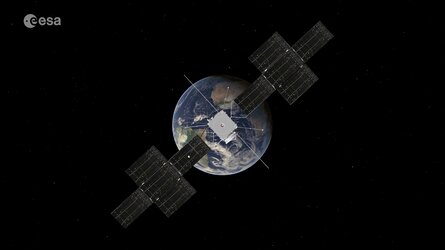
ESA researching atomic layering technique whose inventor won technology's 'Nobel' prize
ESA congratulates its research partner Picosun in Finland, whose board member Dr. Tuomo Suntola was awarded the prestigious Millennium Technology Prize for his invention of an atom-by-atom coating method whose reach extends across daily life.
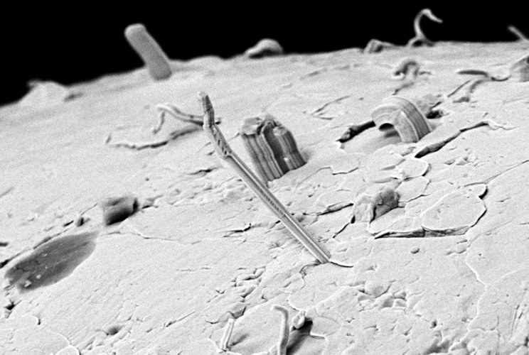
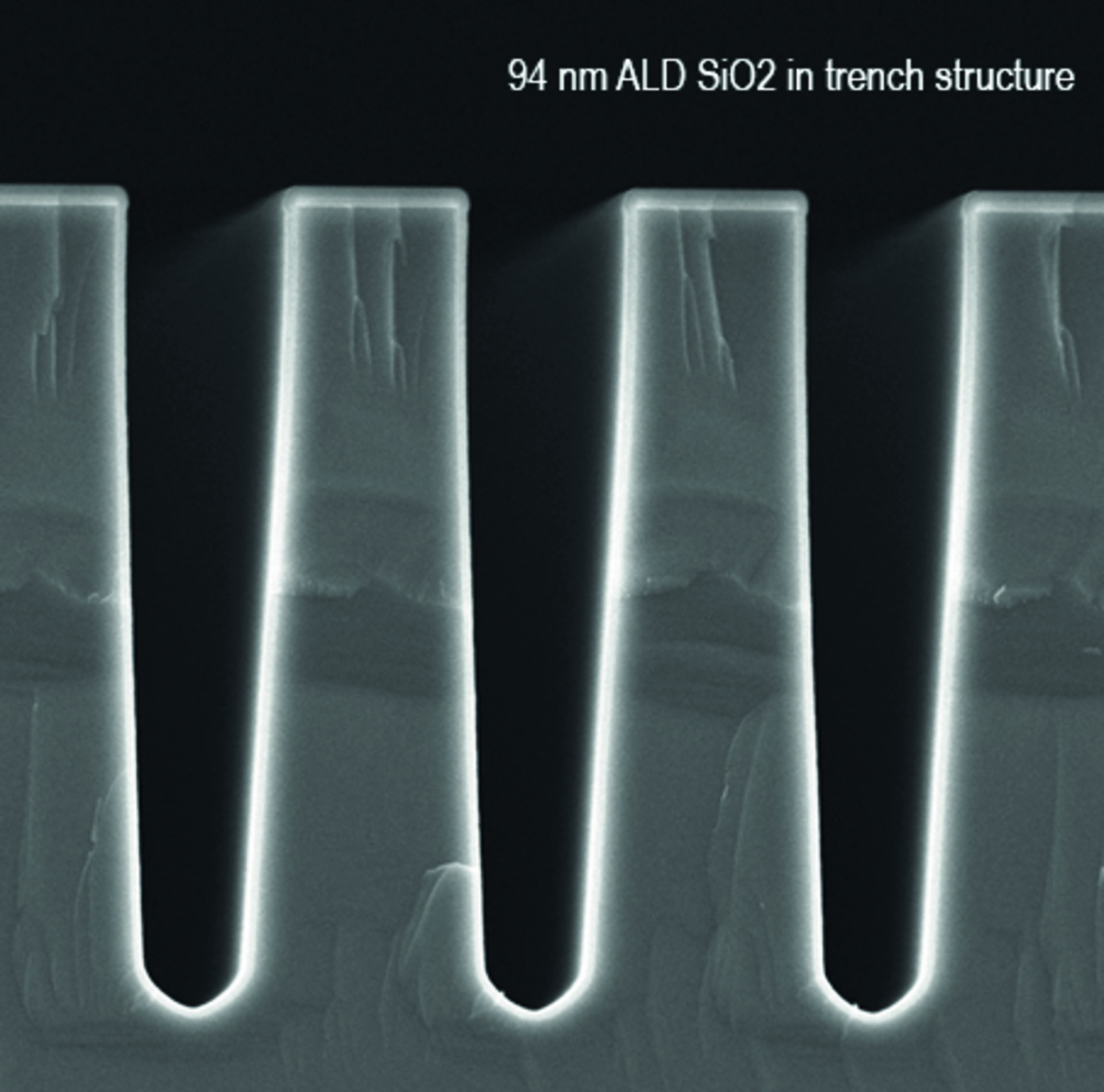
ESA has teamed up with Picosun on the application of this method, called ‘atomic layer deposition’ (ALD) to prevent spontaneous outgrowths from tin solder in circuit boards. Known as ‘tin whiskers’, the electrically-conductive nature of these eruptions has led to the loss of at least one space mission.
“Having researched ALD for tin whisker prevention, we’re moved to our second phase,” explains ESA engineer Jussi Hokka. “We’re now looking into its wider potential for corrosion protection and as a general coating to safeguard electrical parts.
“In the terrestrial arena ALD is already in widespread but almost invisible use, so it is great to see Dr. Suntola recognised with the Millennium Technology Prize in this way.”
The one-million-euro Millennium Technology Prize is one of the world’s largest technology awards, technology's equivalent of the Nobel Prize, to celebrate innovations making a sustainable impact on our quality of life and wellbeing. Previous winners include worldwide web inventor Tim Berners Lee.
ALD involves laying down vaporous coatings onto surfaces a single atomic layer at a time, through the use of alternating ‘pulses’ of materials. The surface becomes entirely saturated in a uniform way before the next layer is added. “The end result is a very uniform surface coating, laid down to an extremely controlled thickness, an atomic layer at a time,” says Dr. Suntola.
“I was recruited by a medical company as a young researcher in the mid-1970s and asked to invent something they could make use of – so I did. I devised ALD as a way of making flat panel displays, at a time when cathode ray tubes remained the standard.
“For the first decade or so my main focus with ALD was to realise that goal, and we eventually ended up providing an electroluminescent display for Helsinki Airport in 1983. They are still manufactured at the same factory for very special applications, such as needing to withstand every low temperatures or vibrations.”

The wider potential of the process was clear, as the range of ALD materials grew steadily. Dr. Suntola went on to work at a subsidiary of the Finnish national oil company, looking into applications including chemical catalysts for oil refining and semiconductor coatings.
“That idea was always there. We had talks with a semiconductor company in the 1980s about using it in integrated circuit manufacturing, but they saw no advantage in it over accepted methods. However, as microelectronics kept on following Moore’s Law into the 21st century – growing smaller in size as their performance increased – the semiconductor industry took it up.”
Chip maker Intel began harnessing ALD for mass production in 2007, helping the company to advance from 65 nanometres (millionths of a centimetre) down to 45 nm-scale integrated circuit production. Rival companies followed suit.
“ALD’s ability to lay down a carefully controlled layer across a wide variety of shapes proved to be the key,” adds Dr. Suntola. “And it delivers five times the insulating ‘dielectric strength’ of sputtering or any other vapour deposition technique. With current manufacturing techniques a single atomic layer can be laid down in about two seconds – the required thicknesses required being also very small.”

In effect, ALD enabled Moore’s Law to go on working, and opened the way to the current smartphone era – with low-size high-power microelectronics mass produced on an economic enough basis to get into the hands of everybody.
“New uses continue to be found for ALD, such as enhancing the performance of solar cells and batteries – in some countries even coins are treated with ALD, to prevent them from tarnishing.”
Tommaso Ghidini, Head of ESA’s Structures, Mechanisms & Materials Division comments: “Finding a workable method of combating tin whiskers – a kind of sickness of metal that remains dimly understood – could have tremendous impacts in both the space and terrestrial sectors, for example in the automotive and aeronautical industry. Moreover, its corrosion protection capabilities could open up a very wide territory of potential applications.
“Considering the game-changing capability of applying ALD to space, I'm very glad to see its inventor being recognised by the latest Millennium Technology Prize, and we, at ESA, are looking forward to continue this very fruitful collaboration with Dr. Suntola and his team.”