


 Germany
 Austria
 Belgium
 Denmark
 Spain
Spain
 Estonia
 Finland
 France
 Greece
 Hungary
 Ireland
 Italy
Italy
 Luxembourg
 Norway
 The Netherlands
 Poland
 Portugal
 Czechia
 Romania
 United Kingdom
 Slovenia
 Sweden
 Switzerland


Control Loop Processor (CLP) Phase 1
| Programme: | GSTP | Achieved TRL: | 4 |
| Reference: | G521-004ED | Closure: | 2017 |
| Contractor(s): | SABCA (DE), Spacebel (BE), IMEC (BE) | ||
The concept of using dedicated deterministic microprocessors in hard-real-time electromechanical control loops (loop rate > 1 kHz) has already been flight proven with the HBRISC2 processor, used on Vega Thrust Vector Control (TVC) and IXV flap control.
The obsolescence of the ASIC technology used for HBRISC2, as well as the desire to generally increase performance, features and flexibility have called for an evolution of the HBRISC2, the Control Loop Processor (CLP). Driving application, at the time of initiation, were the TVC's for Ariane-6 and Vega-C.
Objective(s)
The overall objective of the CLP activity is to develop, validate, qualify, standardize and commercialise a new System-on-Chip (SoC) called Control Loop Processor (CLP) with enhanced processing performance, full IEEE-754 floating point support and state-of-the art spacecraft communication interfaces.
The present activity covers the first phase (CLP Definition and Architectural Design):
- CLP requirements review (SRR) and IP selection
- Architectural Design (leading to PDR):
- Development of the CLP VHDL source code
- Design verification either by simulation and/or prototyping on a commercial FPGA board
- Selection of the ASIC technology
Requirements review and preliminary design of the Software Development Environment (SDE).
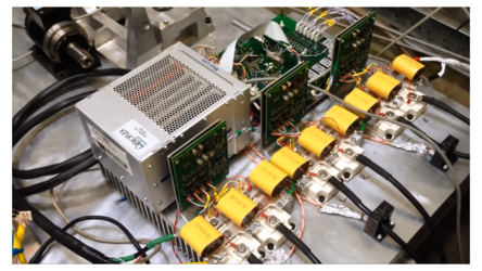
The block diagram of the CLP (compare picture above) shows the two processor (CPU) cores, each having two floating point and one integer unit, as well as a comprehensive set of peripherals and interfaces, connected via an on-chip bus system.
Achievements and status
CLP has been specified, developed in VHDL and verified by an extensive set of test cases. CLP has been implemented on FPGA board and demonstrated in the context of Ariane-6. Initial components of the SDE have been developed.
Trial synthesis on 180 nm DARE ASIC technology from IMEC(BE) has been performed, concluding that a more advanced technology node is required.
Ariane-6 / VEGA-C selected to use the CLP concept for the P120 booster, implemented on commercial FPGA.
The Video (see link on the right side - courtesy of SABCA) demonstrates the CLP, integrated into a commercial FPGA board, controlling a three-phase motor drive electronics. The fault tolerant system continues operating, even when one phase is disconnected.
Benefits
CLP will be beneficial to electromechanical applications demanding high performance and high determinism, e.g.
- TVC on rockets
- Robotics (Rovers, robotic arms)
- Reaction wheels and -spheres for attitude control
Next steps
Phase 2 and 3 have been approved in GSTP, aiming for TRL8 (space qualified component).
Phase 2A in progress (2017) to develop the SDE, providing a full SW tool chain starting from Simulink or C-code, comprising LLVM C-compiler, assembler, configuration generator, trace manager, macro library.
Further development of the CLP ASIC component is subject to availability of a suitable ASIC technology (e.g. DARE-65nm, development just started in another GSTP) and a business case.
CLP Datasheet
If you are interested in the CLP datasheet, please contact Jean-Brieuc.Feron@sabca.be.