Prototyping and Characterization of 1200 V SiC Schottky Diode
| Programme: | TRP Workplan | Achieved TRL: | 4 |
| Reference: | T723-309QT | Closure: | 2013 |
| Contractor(s): | Alter Technology (S), D+T Microelectronica (S), Micross (UK) | ||
The market for TWTA (travel wave tube assembly) pushed towards more power, higher frequency and compact dimensions able to operate at high temperatures. In order to meet the TWTA performances and the power/mass and thermal budget, Schottky diodes capable of withstanding highest voltage, highest operating temperature, low reverse current at high temperature and good switching performances at high frequency are needed. SiC Schottky diodes are therefore the ideal candidate.
Objectives
The objective of the activity was to develop a 1200V SiC Schottky diode in a package suitable for space application. The main goal was to characterize the performances of the devices in terms of switching capability, reliability of the technology and main characterization of static and dynamic parameters as a function of temperatures. The activity also aimed to characterize the tolerance to TID and to heavy ions in order to evaluate their potential future application in space missions.

Achievements and status
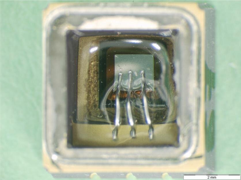
Trade off between different technological solutions have been considered: to meet the stringent electrical requirement in reverse the best topology was the JBS one with a Tungsten Schottky metal. A big challenge was the design of the hermetic package that could be used as drop in replacement of the Si one, to be corona free and able to operate at high temperature.
The evaluation test in term of stability and performances were considered successful. Validation tests of potential users confirmed that the developed diodes exceed the performances they were requiring for prototyping the next generation of EPC. In a second generation, improvement in the reverse current characteristics can be expected by some minor technology adjustments, which would not affect the rest of the characteristics.
The high sensitivity to heavy ions has been confirmed to be the major drawback of SiC Schottky technology for space application. It has been confirmed that heavy ions induce a cumulative degradation of reverse current that can end up in device breakdown. Some mitigations solutions has been identified and need to be verified in future studies.
Benefits
SiC diode is the enabling technology allowing EPCs to work at temperature higher than 65C (the actual max baseplate temperature). It will simplify the thermal design, decrease of distance between EPC and TWT and therefore allowing size and mass reduction. This means reduction of complexity of accommodation of EPC. Finally, it will increase competitiveness of telecom satellites (space segment/satellite equipment).
Next steps
An Artes activity has been proposed and is under approval process “Validation of 1.2KV diode technology in high temperature (95deg) EPCs“ with the goal of to develop and validate at bread-board level a 1.2kV Silicon Carbide (SiC) diode able to tolerate heavy ions radiations, enabling high performance EPC at high temperature. The starting point will be the design already tested in the frame of this TRP, implementing some small modification that should improve the heavy ions tolerance.